Hey everyone, let’s cut to the chase—if you’ve ever worked with tech that needs to bend, flex, or squeeze into tight spaces, you’ve probably encountered rigid flex PCBs. As someone who’s been in the rigid flex PCB game for years now, I get that most folks don’t know what goes into making these things that keep your smartwatch flexible, your aerospace wiring from snapping, or your medical devices small enough to work inside the body. It’s not just a regular PCB with a little tape holding it together, trust me. Let’s walk through the process, straight from the supplier’s side so you get the real deal, not some textbook fluff. Rigid Flex PCB
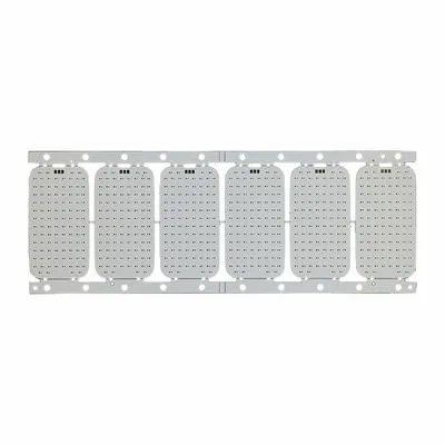
First, let’s get one thing straight: rigid flex PCBs aren’t a single material—they’re a hybrid. Half rigid, half flexible, and the transition zone (that’s where it goes from hard to bendy) is the most important part. Mess that up, and the whole board will crack the second you flex it, or short out when it’s in use. So before we even start building anything, we do a ton of prep work that most people skip over, because if you get this wrong, nothing after matters.
Step 1: Material Selection—This is where we start, not just picking any old copper or resin. Rigid parts usually use FR-4, that standard fiberglass epoxy stuff, but the flexible parts? We use polyimide (PI) or sometimes LCP, depending on the client. PI is the workhorse—cheap, flexible, good temp resistance. LCP is pricier, but better for high-frequency signals, so if it’s a 5G or radar application, that’s what we reach for. For the adhesive, too—we use different ones for different jobs. If it’s medical, we need biocompatible adhesives; if it’s automotive, it has to withstand extreme heat and vibration. Oh, and the copper foil? It’s not just plain copper—we roll it thin for the flex sections, and a bit thicker for the rigid parts because they need to carry more current. We always get certified materials, no cheap knockoffs here—we’ve seen what happens when someone uses subpar PI, and it delaminates after 100 flex cycles. Total waste for everyone.
Step 2: Design & CAD Prep—Wait, this isn’t just drawing lines on a screen. We work closely with clients here, because if their design has a flex zone that’s too narrow, or too many traces in the bend area, it’s a dead board before we lay any copper. We run DFM (Design for Manufacturability) checks on every single order. For rigid flex, the DFM red flags are super specific: how big the flex radius is (rule of thumb, it should be at least 10x the thickness of the flex section), where the transitions are, if there are any vias (those little holes that connect layers) in the flex zone—we don’t do vias there, or they’ll break. We also specify where the stiffeners go—little FR-4 or metal plates glued to the rigid parts so you can solder components without the board bending. This step takes longer than people think, especially for medical or aerospace clients who have super strict specs. We’ve had a client with a wearable insulin pump that needed a flex zone exactly 8mm from the battery pad, so we adjusted their CAD three times before we even touched materials.
Step 3: Lamination—Okay, now we’re getting to the actual building. First, we make the rigid sections and flexible sections separately first, right? Then we bond them together. Wait, no—wait, actually, for multi-layer rigid flex, sometimes we build all layers and then laminate the flex cores into the rigid stack. Let’s clarify: for a basic 2-layer rigid flex, it’s two copper layers on PI, with FR-4 on either side for the rigid bits. For more layers, like 4 or 6, we alternate rigid and flexible cores. The key here is the lamination press. We use vacuum presses, not just regular hot presses, because air bubbles between layers will cause delamination later. We heat it to like 150-180C, apply consistent pressure, and hold it for a set time—too hot, and the PI melts; too cold, and the adhesive doesn’t cure. For the transition zones, we do a “step lamination” so the thickness changes gradually, not abruptly. If you have a hard FR-4 edge right next to thin PI, that’s a stress point waiting to crack. We test the lamination bond strength every batch with a peel test—if the copper or PI pulls apart instead of the adhesive breaking, that’s good.
Step 4: Printing & Etching—This is similar to regular PCB manufacturing, but again, the flex sections are trickier. First, we apply a photoresist layer to the copper surfaces (both rigid and flex parts). Then we use a photoplotter to print the circuit design (the traces, pads, etc.) onto a film, then expose the board to UV light. The parts that get exposed harden, so when we dip the board in etchant, the unexposed copper washes away, leaving the traces. Here’s the catch: on the flex parts, we can’t use harsh etchants that eat away at the PI. We use a gentle, controlled etch specifically formulated for PI-based flex boards. Also, we make sure the traces on the flex sections are a little wider than rigid ones, because thin flex traces break easier when bent. And we double-check all the small pads—if a pad is undersized, when you solder a tiny SMD component, it’ll lift right off. We use automatic optical inspection (AOI) here to catch any mistakes before moving on. No one wants to etch a whole batch wrong because of a flipped trace.
Step 5: Drilling & Plating—Vias are non-negotiable for multi-layer boards, but like I said earlier, no vias in the flex zones. So we mark which areas are rigid and which are flex before drilling. We use high-precision CNC drills, tiny bits—down to 0.1mm diameter for small vias—so we don’t damage the PI. Once drilled, we need to plate the inside of the vias with copper to connect the layers. This is another step that’s different for rigid flex: we use a chemical plating process that doesn’t corrode the flexible PI. After plating, we do a continuity test on every via—if one doesn’t connect, that’s a dud. Also, we add solder mask now, right? Wait, yes, step 5 or 6? Let’s adjust: after drilling/plating, we apply solder mask. For rigid sections, it’s the standard green (or whatever color the client wants) epoxy mask. For flex sections, we use a thinner, flexible solder mask that won’t crack when bent. We leave the flex zones unmasked, actually—because if you mask the PI there, it adds stiffness that ruins the bendability. That’s a common mistake other suppliers make, so we’re careful to mask only the rigid parts and any flex areas that don’t need to bend.
Step 6: Stiffener & Coverlay Application—Wait, coverlay! I forgot that part. Coverlay is the thin, protective film (usually PI with adhesive) that covers the flex traces, like an insulator and a barrier against moisture and dirt. We cut the coverlay exactly to the flex zones—only where it’s needed, not overlapping into rigid parts. Then we align it perfectly, apply heat and pressure to bond it, and laser cut the holes for any pads or connectors. Laser cutting is key here—mechanical cutting would tear the thin PI. Then the stiffeners, like I mentioned earlier: small FR-4 or aluminum plates that we glue to the rigid parts where components get soldered, like the connector pads or battery spots. That way, when you plug a connector in, the rigid part doesn’t flex and break the solder joint. We use a conductive adhesive for stiffeners that carry current, and non-conductive for others. We cure the adhesive in an oven at low temp so we don’t warp the board.
Step 7: Testing & Validation—This is make or break. We don’t just test for continuity, like regular PCBs. For rigid flex, we do flex testing—we put the board in a machine that bends it thousands of times (usually 10,000 to 100,000 cycles, depending on the specs) and check for open circuits or shorts during and after. For medical clients, we do biocompatibility tests if the board touches tissue. For aerospace, thermal cycling tests to make sure it works at -55C to 125C. We also do X-ray inspection for hidden defects in vias, because you can’t see those with the naked eye. And if the client is making a product that’s going to be in a car or something with lots of vibration, we do vibration testing too. We reject any board that doesn’t pass—no cutting corners here, because a failed rigid flex PCB in a pacemaker or a car is way worse than a scrap board.
Step 8: Final Trimming & Packaging—Last step! We trim the board to the exact shape the client needs, using laser cutting again for clean edges (no frayed PI). We also add any final markings—part numbers, logos, etc. Then packaging is super important. We use anti-static, flexible packaging to ship the boards, because if you bend them too hard during shipping, they’ll break. We don’t put them in regular boxes that cram them together—we use individual trays, or roll them gently for very flexible boards. And we make sure to include a test report with every batch, so the client knows exactly what passed, what tests were done, and that it’s ready for assembly.

Now, if you’re someone who needs rigid flex PCBs for medical, automotive, aerospace, wearables, or even industrial equipment—trust me, not all suppliers do this process right. Skimp on lamination, or use cheap coverlay, and you’ll end up with boards that fail after a few uses. We’ve been doing this for years, so we know the ins and outs, the little details that make a good rigid flex board vs. a bad one. If you’re looking for a reliable supplier, hit us up to talk through your project—whether you need a small batch for a prototype or a large order for full production, we can work with you to get exactly what you need, no weird hoops to jump through.
Flex PCB References:
- "Rigid-Flex PCB Design and Manufacturing: A Practical Guide," IPC Association Connecting Electronics Industries
- "Flexible and Rigid-Flex Circuit Technology," Rogers Corporation
- Medical Device Manufacture of Rigid-Flex Printed Circuit Boards, Journal of Electronic Materials
- "High-Frequency Rigid-Flex PCBs for 5G Applications," Taiyo Yuden Technical Note
- Automotive-Grade Rigid-Flex PCB Reliability Testing, SAE International
Huaswin Electronics Technology Co., Ltd.
Address: Building A2, Hao Hai Hong Industrial Park, No.3 Yu He Road, Gong He, Sha Jing, Bao An, Shenzhen
E-mail: sales@huaswin.com
WebSite: https://www.huaswin-pcba.com/
